How to Design PCBs Part 2

As promised in my previous post here is the completion of my first foray into the world of PCB design. Here I will go through installing the components and testing the boards.

The Boards

The backside of the PCB

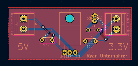
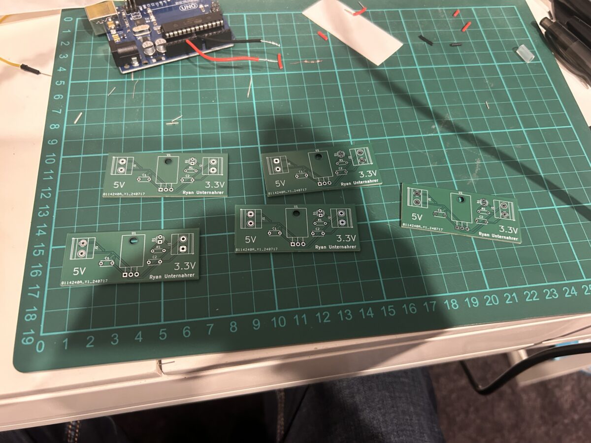
The shipping of the boards was quicker than I expected and only took about 10 days from purchase to arrival which was the lower end of JLCs estimate. They were well-packaged and the silk screen printing was all correct. These PCBs were 2 layer copper boards with an FR4 core. Furthermore, all the holes and vias were in the proper positions.

Installing Components

PCB with components installed.

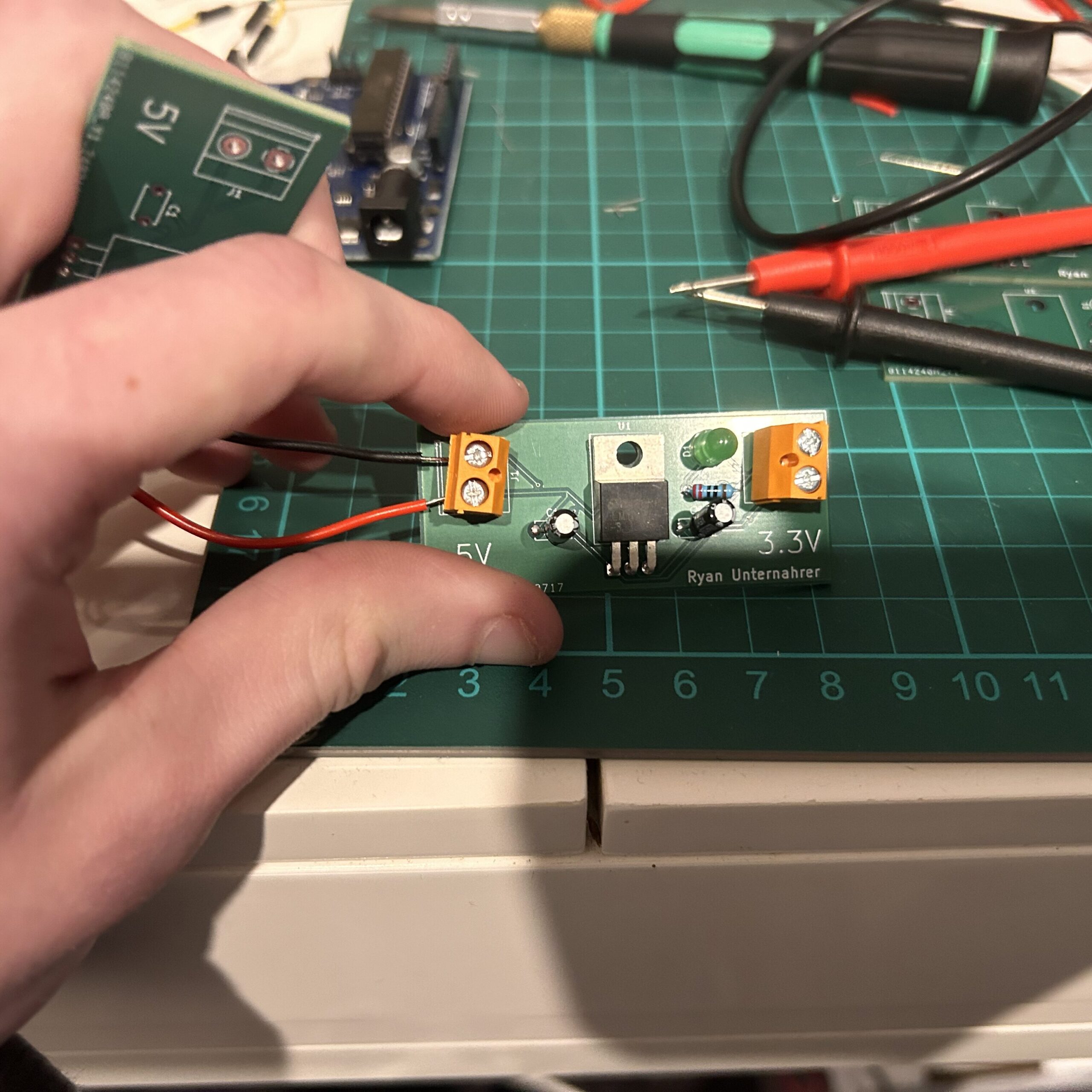
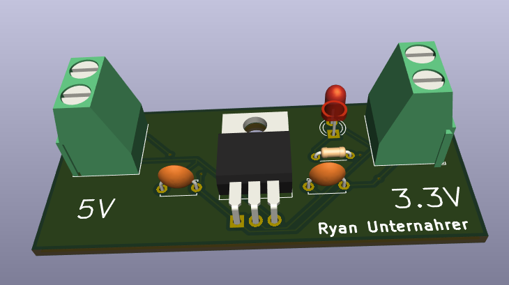
I then installed the components on the board. The component holes were slightly larger than I expected. That led to a small amount of solder leakage over to the front side of the board though it was minimal. The footprint for the MOSFET was perfect and the mounting hole lined up perfectly. I also got lucky that the footprint for the screw terminals was right. I did not check it before purchase which was probably not a great idea.

Testing

Testing the board.

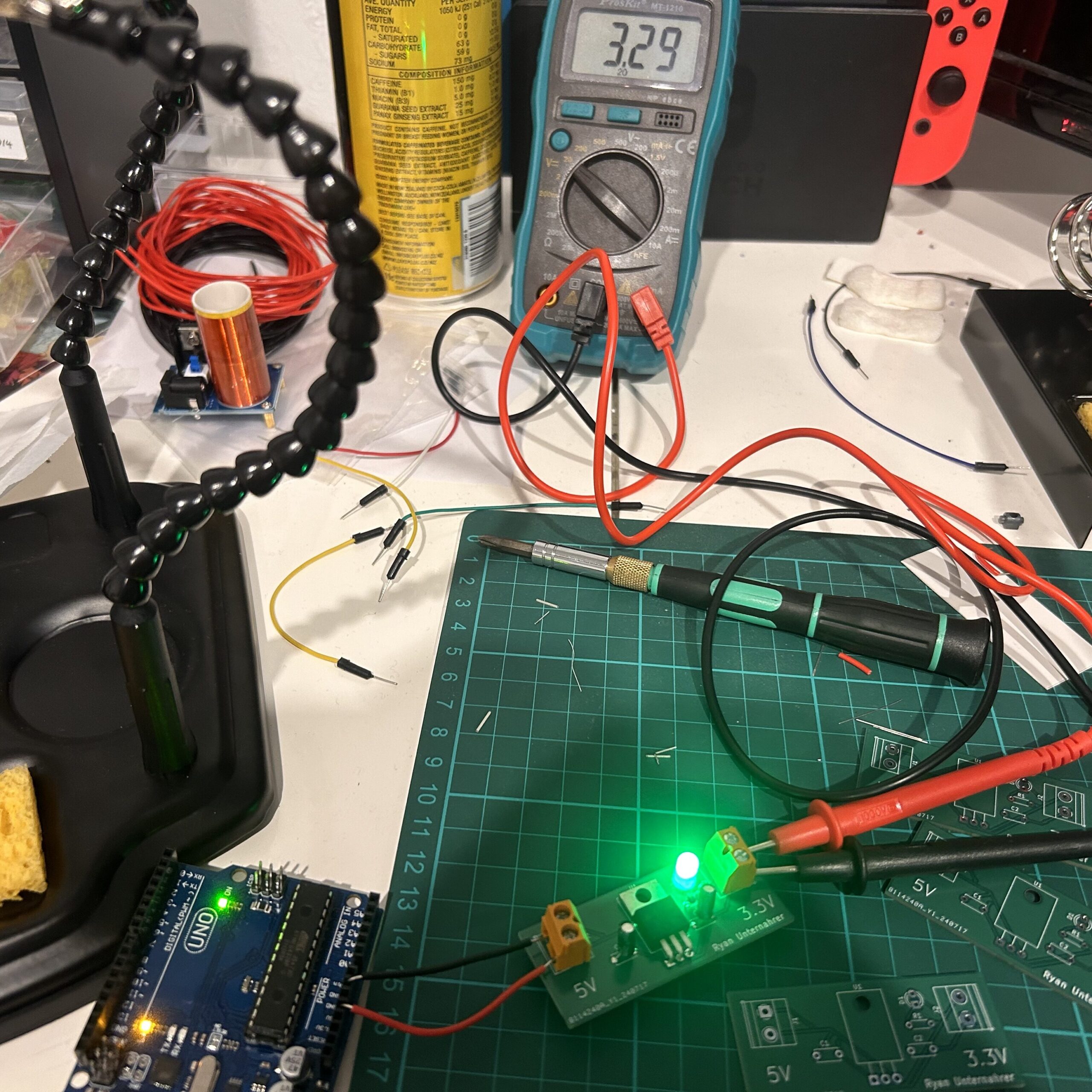
After installing all the components it was time for the moment of truth. Testing that after applying a 5V input to the board we would get a 3.3V output. As can be seen above that is the case. I was somewhat surprised that this was the case as I was expecting that I had made some mistakes with the design. I would make a few changes if I were to do this again though. One change I would label the positive and negative on the terminals using silkscreen. Another change would be to increase the resistance on the LED as it seems the 220Ω resistor was not quite enough and the LED was running quite bright.

Conclusion

This project has been one of the more interesting ones I have undertaken recently. I am going to make some more boards in the future. The success of this project has increased my confidence in electronics and I am excited for my next project. However, it may be a while before my next one as the University semester has started once again.

How to Design PCBs Part 1

I have always had an interest in electronics since my Grandfather introduced the hobby to me. But over the past few years, I haven’t been as active as I once was. After a night of YouTube browsing, I found myself drawn back in and decided to teach myself Print Circuit Board (PCB) Design. This stuff is different from my normal work in the software world but is an interesting learning opportunity.

Introduction

After some research and experimentation, I decided to use the open-source software package KiCAD for my design of circuits and PCBs. I found KiCAD to have numerous resources online. It is a fully featured package for circuit and PCB design that includes symbol and footprint editors. I learnt most of the basics from this video on YouTube but the forums are very active and helpful if you have specific questions.

The Circuit

Schematic of the voltage regulator.

After some time learning about the software, I decided to create a simple circuit for fabrication. Many standard power supply methods for microcontrollers use 5V. On the other hand, my Raspberry Pi Pico and many of its components use 3.3V. So I decided to create a voltage regulator.

The main component of this is the LM1117 specifically the 3.3 variant. This takes an input voltage of 1.2 to 13.8V input and outputs 3.3V. Texas Instruments also recommends a 10uF capacitor to improve the consistency of power and reduce any noise in the circuit. So I placed one of these each on the input and output. I also added an indicator LED on the output.

I/O

For input and output, I had to decide how I would input and output power from the device. The three main options I considered were pins/sockets, soldered connections, and screw terminals.

Pins and sockets are both commonly used in the world of microcontrollers and are well-suited to hobbyist and prototyping projects. They are also the IO method for many of my microcontrollers and components. However, they lack the durability and stability needed for use in more permanent projects.

Soldered connections are the most permanent and cost-effective option. But their permanence is also their biggest drawback. For a hobbyist like myself constantly having to resolder these to each project will quickly become a hassle as I jump from project to project, prototype to prototype.

The final option was screw terminals. They are the most expensive option, the ones I am using are $1.90 each, but they strike a balance between the permanence of soldered connections and the ease of change in pins. Therefore I decided to use screw terminals for this project.

Layout

Final Version of layout.

After I designed the circuit and chose the components that would be used I imported the footprints into the PCB layout software that is a part of KiCad. I decided to use a 2-layer PCB as it provides flexibility in layout. I ended up making use of this to allow traces to cross one another.

Fabrication

JLC’s model of my PCB.

For fabrication, I decided to use JLC PCB as they are both cheap and seem to have a good reputation among hobbyists. For this, I had to generate Gerber and Drill files for them. I found KiCAD made this very easy and after uploading the files and setting a few options my PCBs were ordered. In total including shipping, this cost me only $5.67 which I consider an exceedingly reasonable price for 5 PCBs printed and shipped when working on this small of an order size.

Conclusion

To conclude, I have found this project to be one of the most engaging side projects I have done in recent times. It has greatly boosted my confidence in electronics. I have learnt a great many new skills and I hope to learn more soon. I will post an update when I receive the boards going through my assembly and testing of the boards.

Side-Channel Attack on LLC

Introduction

This semester I am taking a Cyber Security class and for the final assignment, I was tasked with performing a side-channel attack on a computer’s LLC(Last Level Cache).

Much like the last assignment to simulate quantum key encryption, there are two parts to the assignment. I was to create both a program and write a short report on the assignment. My report should cover both the theory behind the attack and the effectiveness of the program I created. To write the report I used LaTeX as I have found it to be a very effective tool this semester. I am writing the program for this assignment in Java though most languages should be effective.

What is a Side-Channel Attack?

First off I should explain what a side channel attack is. A side-channel attack is a method by which one can infer information about a computer or a program using indirect methods. If you want to learn more about side-channel attacks I would highly recommend reading about the Meltdown and Spectre vulnerabilities. The example for this assignment is inferring the size of the LLC of a computer’s CPU. Therefore to perform a side channel attack I must find an indirect way to infer the size of a computer’s LLC.

My Side-Channel Attack

After reading the article we were provided with when given the assignment I then decided on using differently sized arrays. I will measure the time needed to access data in the array and this should allow me to infer the cache size. I will step through the different sizes of arrays and measure a value for each. Plotting these values should allow me to see a spike in time which means we are having cache misses.

I used arrays from 1Kb in size up to 64Mb doubling at each step. For each size I will run 100 tests, each test will consist of incrementing values in the array 1 million times. Each test will be timed and the times for each size will be averaged. This should allow us to get an accurate value for each size without running into any outliers.

We will use two different methods to determine which element of an array we access. A random method, and a sequential method. This is another requirement of the assignment is that I test multiple methods for my attack.

Side-Channel Attack output
Output of Random Access Side-Channel Attack

The Report

I wrote a short report (5-page limit) on my methodology for the attack and the results I got from said attacks. I wrote this report using LaTeX as I have found it to be a very useful tool this semester. Included in the report were graphs of my results and an analysis of my results for each method. If you wish to read it in full the PDF is available below.

Disclaimer

Though it should go without saying I will say. This is all for purely educational purposes. Do not run software of this kind on any systems you do not have permission to use. Also, ensure when testing software of this kind you are doing so in a secure environment and are in compliance with all local laws and regulations.