As promised in my previous post here is the completion of my first foray into the world of PCB design. Here I will go through installing the components and testing the boards.
The Boards

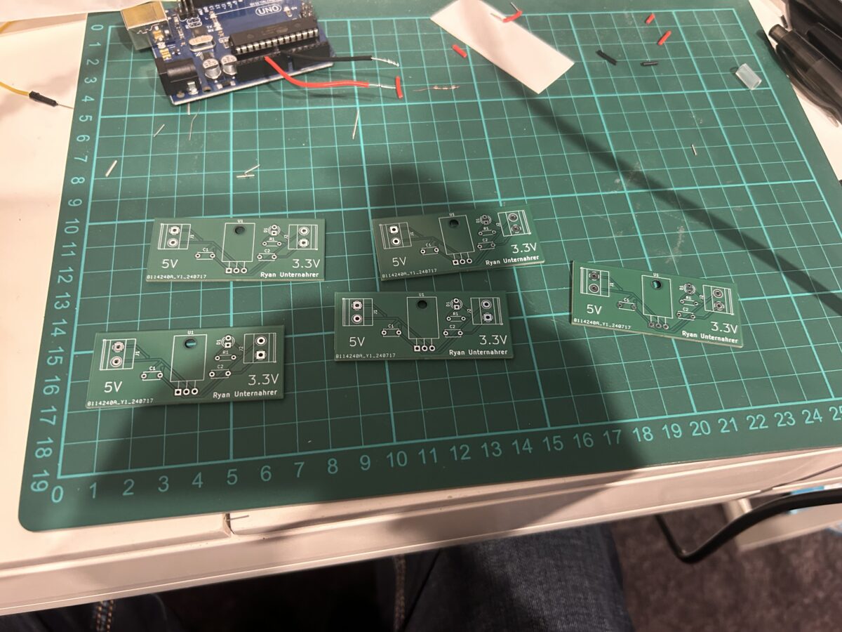
The shipping of the boards was quicker than I expected and only took about 10 days from purchase to arrival which was the lower end of JLCs estimate. They were well-packaged and the silk screen printing was all correct. These PCBs were 2 layer copper boards with an FR4 core. Furthermore, all the holes and vias were in the proper positions.
Installing Components

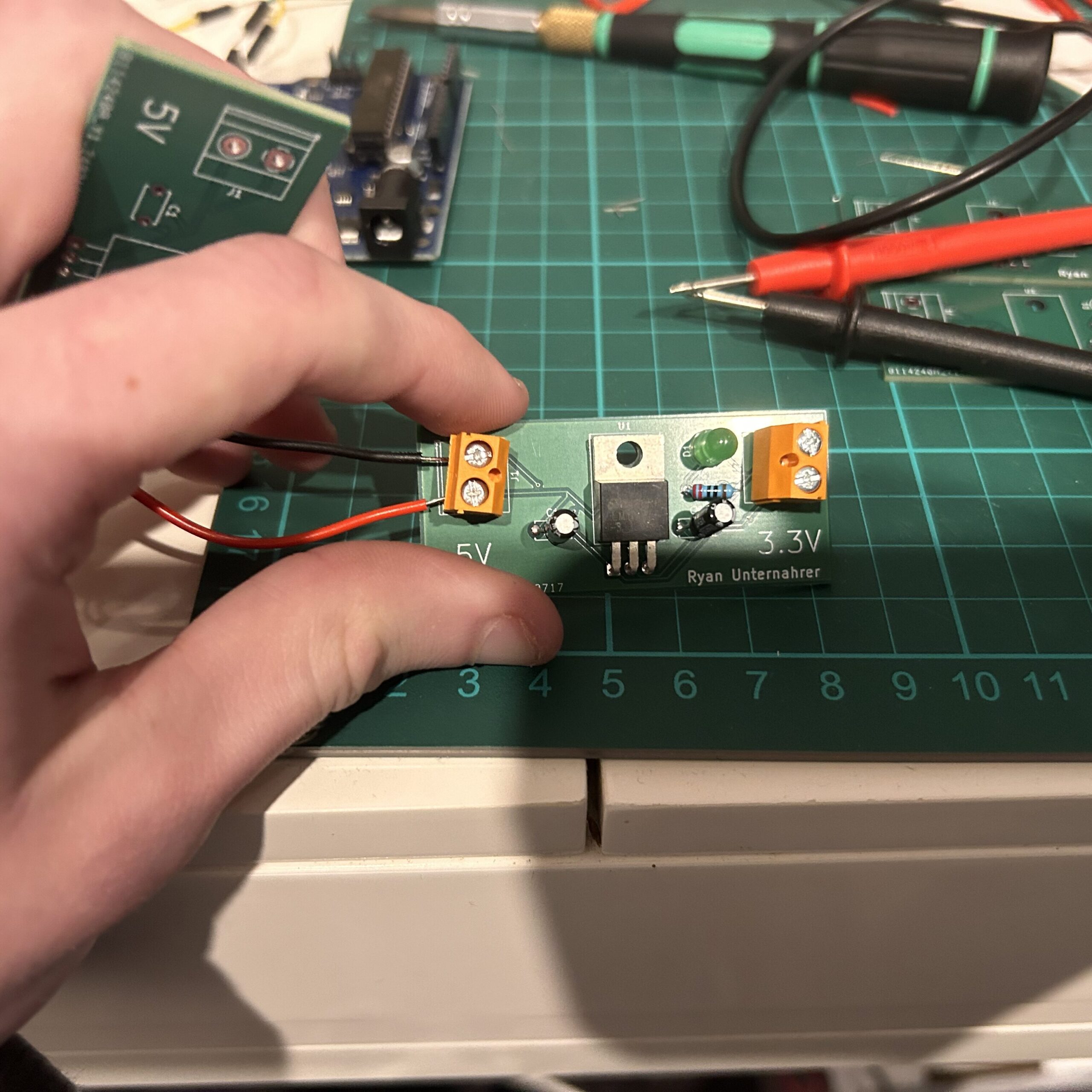
I then installed the components on the board. The component holes were slightly larger than I expected. That led to a small amount of solder leakage over to the front side of the board though it was minimal. The footprint for the MOSFET was perfect and the mounting hole lined up perfectly. I also got lucky that the footprint for the screw terminals was right. I did not check it before purchase which was probably not a great idea.
Testing

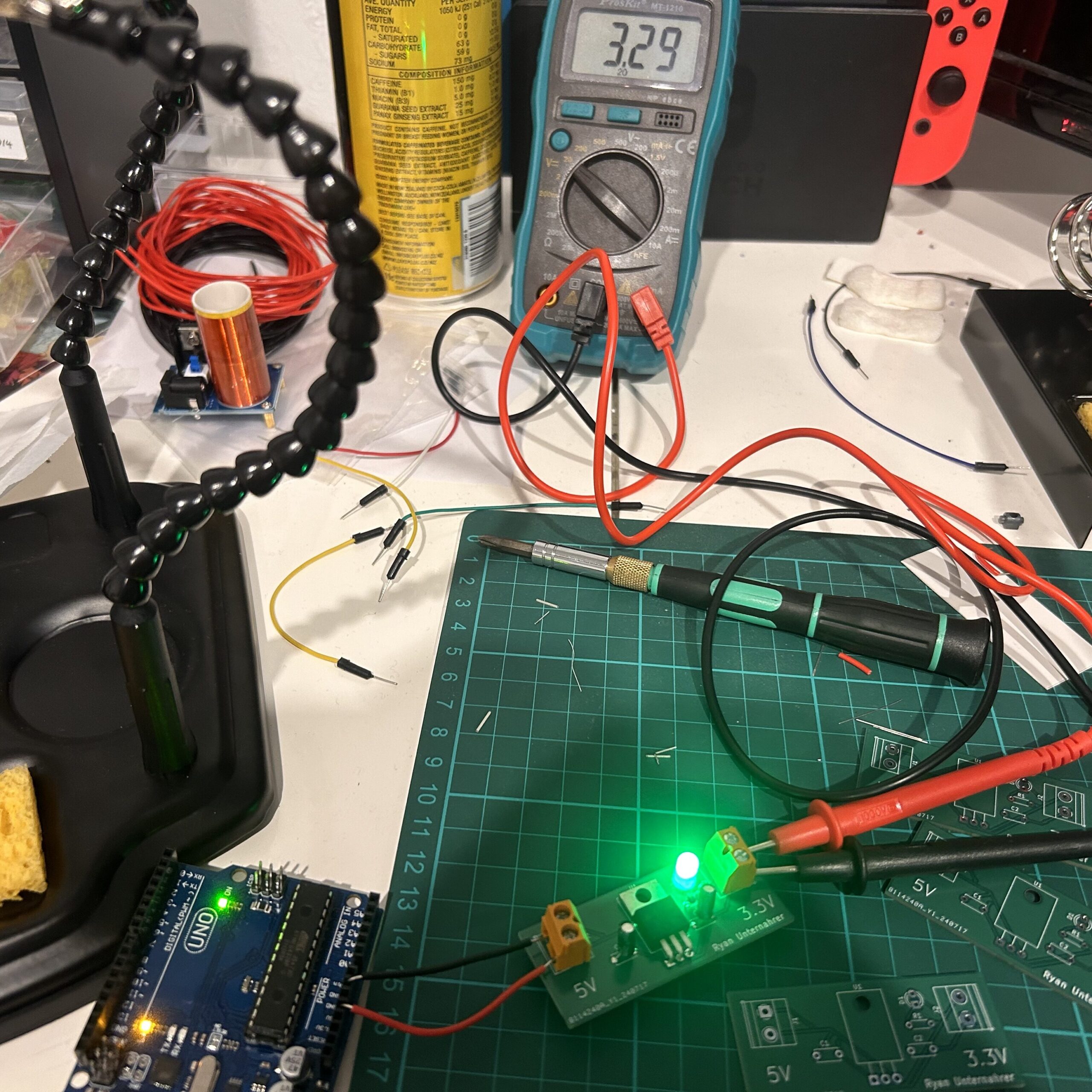
After installing all the components it was time for the moment of truth. Testing that after applying a 5V input to the board we would get a 3.3V output. As can be seen above that is the case. I was somewhat surprised that this was the case as I was expecting that I had made some mistakes with the design. I would make a few changes if I were to do this again though. One change I would label the positive and negative on the terminals using silkscreen. Another change would be to increase the resistance on the LED as it seems the 220Ω resistor was not quite enough and the LED was running quite bright.
Conclusion
This project has been one of the more interesting ones I have undertaken recently. I am going to make some more boards in the future. The success of this project has increased my confidence in electronics and I am excited for my next project. However, it may be a while before my next one as the University semester has started once again.

